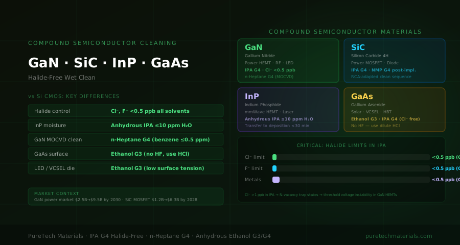
Compound semiconductor devices — including gallium nitride (GaN) power transistors, silicon carbide (SiC) MOSFETs, indium phosphide (InP) high electron mobility transistors (HEMTs), and gallium arsenide (GaAs) multijunction solar cells — represent the fastest-growing segment of the semiconductor industry. Unlike silicon CMOS, compound semiconductor fabrication involves III-V and IV-IV substrates with unique chemical compatibility requirements that demand careful selection of cleaning solvents.
Why Compound Semiconductors Need Special Cleaning Chemistry
Compound semiconductor surfaces are far more chemically reactive than silicon. The issues specific to each material:
| Material | Key Concern | Problematic Impurities |
|---|---|---|
| GaN on Si or SiC | Surface pitting; Ga-OH bond formation | Cl⁻, F⁻ in cleaning solvents |
| SiC (4H-SiC) | Native oxide quality; interface state density | Metallic contamination; organic residue |
| InP | Phosphide oxidation; indium hydroxide formation | O₂, H₂O; acidic/basic pH excursions |
| GaAs | Arsenic surface oxidation; galvanic corrosion | Cl⁻; Fe, Cu (galvanic couple formation) |
GaN Power Device Cleaning Requirements
GaN power transistors (HEMT, GaN-on-SiC, GaN-on-Si) operate at high electric fields where even sub-monolayer surface contamination creates trap states that degrade electron mobility and cause current collapse. Wet cleaning requirements for GaN fabrication:
IPA for GaN Substrate and Epitaxial Wafer Cleaning
Electronic grade G4 IPA with ultra-low halide content (Cl⁻ <0.5 ppb, F⁻ <0.5 ppb by IC) is the primary cleaning solvent for GaN substrate surfaces before MOCVD epitaxial growth. Chloride contamination at GaN surfaces creates N-vacancy trap states that cause threshold voltage instability in GaN HEMTs. Even Cl⁻ at 1 ppb concentration in rinse IPA can cause measurable surface potential variation on AlGaN/GaN heterostructures.
n-Heptane for GaN MOCVD Reactor Cleaning
GaN MOCVD (metal-organic chemical vapor deposition) reactors use trimethylgallium (TMGa) and ammonia (NH₃) as precursors. Between growth runs, the quartz reactor liner and susceptor require organic cleaning to remove GaN particulates and TMGa decomposition products. Electronic grade n-heptane (G4, total aromatics ≤10 ppm, benzene ≤0.5 ppm) is specified because aromatic impurities from lower-grade hexane or heptane deposit as carbon contaminants on the heated susceptor surface, nucleating growth defects in subsequent GaN epitaxial films.
SiC MOSFET Cleaning Chemistry
4H-SiC power MOSFETs require an exceptionally clean SiO₂/SiC interface to achieve acceptable channel electron mobility (target: >50 cm²/V·s vs. <20 cm²/V·s for typical SiC oxide quality). Standard RCA cleaning (SC-1, SC-2, HF dip) is used, with IPA G4 for all final rinse steps after the HF oxide strip.
Post-Ion-Implant Cleaning
SiC MOSFETs use nitrogen or aluminum ion implantation for N⁺/P⁺ source/drain regions. Post-implant resist strip uses NMP G4 (for thick resists at elevated temperature), followed by G4 IPA rinse. The NMP metal content (Fe ≤0.2 ppb) is critical because iron contamination at the implant-damaged SiC surface creates deep-level traps that reduce minority carrier lifetime in bipolar SiC devices.
InP HEMT Cleaning
InP-based HEMTs for millimeter-wave (mmWave) and terahertz applications require extremely low surface contamination for gate recess etching and ohmic contact formation. InP is uniquely sensitive to moisture — even brief exposure to humid air forms indium hydroxide (In(OH)₃) islands that degrade ohmic contact resistance by 50–100%.
Anhydrous IPA Cleaning Protocol
Anhydrous G4 IPA (≤10 ppm H₂O) is used for all InP surface cleaning steps immediately before gate metal deposition. The anhydrous specification prevents In(OH)₃ formation during the cleaning process. The cleaned InP surface is transferred to the deposition system under N₂ within 30 minutes.
GaAs and AlGaAs Solar Cell Fabrication
III-V multijunction solar cells (GaInP/GaAs/Ge) achieve efficiencies of 30–47% in concentrated solar applications. GaAs substrate cleaning before epitaxial growth uses a sequence analogous to silicon RCA, with critical modifications:
- Organic degreasing: Ethanol G3 (≤0.5 ppb total metals) removes surface hydrocarbons from wafer handling without leaving halide residues that etch the GaAs surface.
- Oxide removal: Dilute HCl (not HF — HF attacks GaAs preferentially at Ga-As bonds) removes the native GaAs oxide.
- Final rinse: G4 IPA (≤0.1 ppb Cl⁻) prevents chloride re-adsorption on the freshly etched GaAs surface before loading into the MOCVD reactor.
LED and VCSEL Device Cleaning
Vertical-cavity surface-emitting lasers (VCSELs) and high-brightness LEDs use GaN, AlGaAs, and InGaP epitaxial structures. Electronic grade ethanol (G3, ≤1 ppb total metals) is the standard cleaning solvent for LED chip surfaces before bond wire attachment and encapsulation. Ethanol's low surface tension and rapid evaporation rate (BP 78°C) make it preferable to IPA for LED die surfaces where residual solvent causes optical absorption.
Conclusion
Compound semiconductor wet cleaning requires careful attention to halide impurities (Cl⁻, F⁻) in cleaning solvents — particularly IPA and hydrocarbon solvents. G4 IPA with Cl⁻ ≤0.5 ppb is the baseline specification for GaN and GaAs substrate cleaning. n-Heptane G4 with ≤0.5 ppm benzene and ≤10 ppm total aromatics is specified for GaN MOCVD reactor cleaning. Anhydrous IPA (≤10 ppm H₂O) is required for InP device processes.
Tags
Related Search Topics
PureTech Materials — Technical Team
Practical technical content for buyers, quality teams and process specialists comparing high-purity chemical specifications, qualification evidence and supply routes. Product claims remain subject to the current controlled specification and project review.