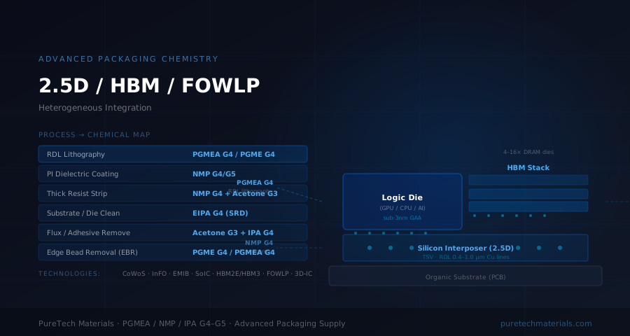
Advanced and heterogeneous packaging has emerged as the industry's primary vehicle for continued performance scaling after Moore's Law slows at the transistor level. Technologies including fan-out wafer-level packaging (FOWLP), high-bandwidth memory (HBM), 2.5D silicon interposers, chip-on-wafer (CoW), and full 3D-IC stacking all rely on precision wet chemical processes with stringent solvent purity requirements.
The Advanced Packaging Chemical Landscape
Unlike front-end-of-line (FEOL) processes which use aggressive mineral acid and oxidant chemistry, advanced packaging wet processes are dominated by organic solvents for polymer deposition, photoresist patterning, and contamination control. The key solvents and their roles:
| Solvent | Grade | Primary Application |
|---|---|---|
| PGMEA | G4/G5 | RDL photoresist primary solvent; PI precursor; EBR |
| PGME | G4 | EBR co-solvent; resist dilution; ARC coating |
| NMP | G4/G5 | PI precursor dissolution; thick resist strip; BCB |
| IPA (electronic) | G4 | Substrate cleaning; post-etch rinse; SRD |
| Acetone | G3/G4 | Pre-clean; flux removal; adhesive clean |
| Butyl acetate | G4 | Negative-tone developer for thick PI resist |
Fan-Out Wafer-Level Packaging (FOWLP)
FOWLP (including TSMC's InFO, ASE's FoCoS, and Amkor's SWIFT) embeds bare dies in a reconstituted wafer of epoxy molding compound, then builds redistribution layers (RDL) on the flat reconstituted surface. RDL line widths in leading FOWLP processes are 2–5 μm, requiring photolithography with i-line or laser direct imaging (LDI) resists.
RDL Lithography Solvents
PGMEA (G4, ≥99.99% purity) is the primary solvent for thick positive photoresists (10–30 μm) used in RDL copper plating mask applications. The thick film requires a high-viscosity resist formulation with 40–55% (w/w) polymer in PGMEA. PGME is added as a co-solvent (10–20% of total solvent) to reduce viscosity and improve spin-coating uniformity across the 300mm reconstituted wafer.
Epoxy Molding Compound Cleaning
Epoxy mold flash on die surfaces must be removed before RDL deposition. Acetone G3 grade is commonly used for plasma-enhanced wet cleaning, followed by G4 IPA rinse and N₂ spin-dry.
High-Bandwidth Memory (HBM) Stacking
HBM stacks 4–16 DRAM dies using through-silicon vias (TSV) and micro-bump bonding. TSV fabrication uses deep silicon etching followed by barrier/seed layer deposition and electrochemical copper fill — each requiring organic solvent cleaning between steps.
TSV Post-Etch Cleaning
After deep reactive ion etching (DRIE) of TSV holes (diameter 5–10 μm, depth 50–100 μm), photoresist residues and etch by-products must be removed without damaging the high-aspect-ratio silicon structures. NMP G4 at elevated temperature (80°C) is used for positive thick photoresist stripping. G4 IPA rinse (≤10 ct/mL at ≥0.5 μm) prevents particle redeposition in the high-aspect-ratio vias.
2.5D Silicon Interposer
2.5D integration places multiple chiplets (logic, HBM, I/O) on a passive silicon interposer with fine-pitch RDL (0.4–1.0 μm Cu lines) connecting them. TSMC's CoWoS (Chip-on-Wafer-on-Substrate) and Intel's EMIB are leading implementations. The silicon interposer is fabricated using full front-end lithography processes, requiring the same PGMEA/PGME photoresist solvents as logic wafer fab.
Organic Redistribution Layer on Interposer
Some 2.5D implementations use organic build-up film (ABF) instead of silicon interposers. ABF lamination and patterning requires NMP G4 for dry-film photoresist stripping and G4 IPA for post-strip rinse and substrate clean before next-level lamination.
Polyimide (PI) as Advanced Packaging Dielectric
Polyimide is the dominant stress-buffer and inter-metal dielectric in advanced packaging because of its low modulus (reduces CTE mismatch stress), excellent electrical properties, and thermal stability to 350°C. PI is deposited from a polyamic acid precursor dissolved in NMP at 15–30% (w/w) concentration.
NMP G5 for PI in Fan-Out Applications
Fan-out processes use very thin PI layers (2–10 μm) for stress relief over molding compound. Metallic contamination in NMP transfers to the PI film and can cause local dielectric breakdown at breakdown fields below specification. G5 NMP (total metals <0.1 ppb) is increasingly specified for high-reliability automotive and AI accelerator FOWLP applications.
Substrate Cleaning and Final Rinse
All advanced packaging substrates require a final clean before flip-chip bonding or wire bonding to remove organic contamination, flux residues, and particles. G4 IPA (≤10 ct/mL, ≤0.5 ppb total metals) in a megasonic spray-clean or immersion system achieves the surface cleanliness required for high-reliability solder joint formation.
Conclusion
Advanced packaging processes require a tailored solvent portfolio: G4/G5 PGMEA for RDL lithography, G4/G5 NMP for PI precursor and resist stripping, and G4 IPA for substrate cleaning and post-process rinse. As heterogeneous integration scales to sub-2μm RDL and drives toward 3D stacking of memory and logic, solvent purity requirements will continue to tighten toward G5 specifications across all process steps.
Tags
Related Search Topics
PureTech Materials — Technical Team
Written by process engineers with hands-on experience in semiconductor wet clean, lithography, advanced packaging, and battery manufacturing. PureTech provides SEMI C1 certified electronic grade chemicals for fabs, OSATs, and battery manufacturers worldwide.